
Intermediate · visual course

PCB Design

PCB design translates an electrical idea into exact physical layers that a manufacturer can build and inspect.

EAGLEKiCadElectronics 4 guided sessions 8 skill tracks 3 example projects
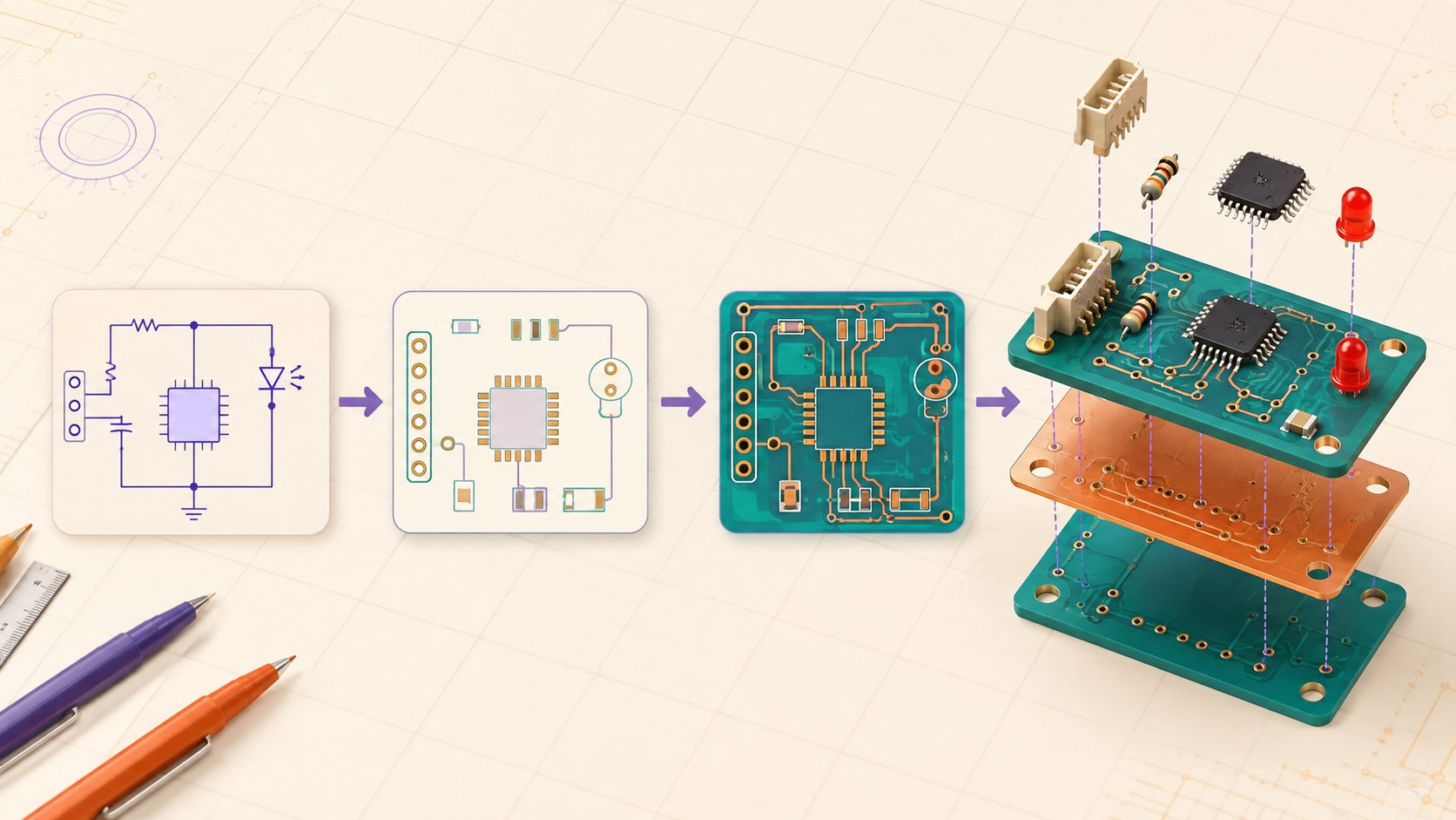
Three-dimensional PCB workflow from schematic and footprints to routed copper layers and assembled board
Concept overview · generated for this Academy4Tech lesson
Start here

See the system, then build it.

A beautiful layout cannot repair a wrong schematic. Check electrical intent before arranging the board.

01Explain schematic symbols, nets, footprints and pads
02Place components using electrical and mechanical needs
03Route power, signals, planes and vias thoughtfully
04Run ERC and DRC before creating fabrication files
Your progress Keep your learning momentum going

0 of 4 sessions complete

Interactive 3D learning studio

PCB layout studio

Move from electrical intent to footprints, copper and checks for a manufacturable board.

Interactive system model · loads on request Poster mode
Explore the system in 3D Inspect the labelled subsystems and watch their modelled process. The lesson flow beside it is a separate conceptual sequence unless it explicitly names the same subsystem. The poster remains available if WebGL is unsupported.
Selected lesson · conceptual flow

From idea to schematic

What information belongs in a schematic?

Step 1 of 4 · Requirement

Step through this lesson’s conceptual sequence here. Inspect the separate 3D subsystem model below it to understand the system’s structure.

3D subsystem inspector · 4 model parts
Mini experiment

Change one variable. Predict first, then test.

Choose 0.25–0.60 mm for this simplified signal.

0.35 mm
Live result Move the control to test your prediction

Choose 0.25–0.60 mm for this simplified signal.

Every highlighted 3D group corresponds to a labelled system part. A slider changes the model only when that relationship can be represented faithfully; otherwise the geometry stays still and the live calculation explains the effect. The model simplifies scale and geometry, so use the lesson’s safety notes, measurements and official documentation when building a real system.

01
Session 1 · 20 min

From idea to schematic

What information belongs in a schematic?

Understand it

A schematic describes components and electrical connections, not their physical positions. Symbols represent parts, pins are connection points, and nets join pins that must be electrically common. Clear labels make intent reviewable.

Interactive concept flow

Step 1 of 4 Requirement

Choose a step to inspect it, or run the complete sequence.

Sequence progress
1 / 4
Picture it

A useful analogy

A subway map explains which stations connect even though it does not copy the city’s exact geography.

Apply it

Worked example

Draw a connector, resistor and LED in series; label power and ground and assign realistic values.

Try it
  1. Draw a battery-resistor-LED schematic.
  2. Mark polarity and current path.
  3. Have a partner find one possible wiring error.
Quick checkDoes schematic position determine board position?

Answer: No. The schematic shows electrical relationships; physical placement happens in the PCB layout.

02
Session 2 · 25 min

Footprints and placement

How does a symbol become a physical component?

Understand it

A footprint contains copper pads and mechanical information that match a real part. Package dimensions, pin numbering and orientation must match the datasheet. Placement begins with board shape, connectors and mechanical constraints, then groups related components.

Interactive concept flow

Step 1 of 4 Symbol

Choose a step to inspect it, or run the complete sequence.

Sequence progress
1 / 4
Picture it

A useful analogy

A furniture plan must use the real dimensions and doorway positions, not just a list of furniture.

Apply it

Worked example

Place a decoupling capacitor close to the microcontroller power pin and keep connectors accessible at the edge.

Try it
  1. Compare one symbol with two possible footprints.
  2. Use dimensions to choose the right one.
  3. Mark pin 1 on both.
Quick checkWhy verify a footprint against the datasheet?

Answer: A wrong pad size, spacing or pin order can make the manufactured board unusable.

03
Session 3 · 25 min

Copper, layers and routing

How do physical tracks change circuit behaviour?

Understand it

Tracks have resistance and carry current. Width, length, spacing and return path matter. Plan power first, use ground zones where appropriate, keep sensitive signals away from noisy switching paths, and use vias to change copper layers.

Interactive concept flow

Step 1 of 4 Place by function

Choose a step to inspect it, or run the complete sequence.

Sequence progress
1 / 4
Picture it

A useful analogy

Road width and route affect how much traffic can move and how different traffic streams interfere.

Apply it

Worked example

Use a wider power track for a motor load and keep its high-current return away from a small analog sensor path.

Try it
  1. Colour power, ground and signal nets differently on a printed layout.
  2. Find a long return path.
  3. Propose a shorter arrangement.
Quick checkWhat is a via?

Answer: A plated hole that electrically connects copper between PCB layers.

04
Session 4 · 30 min

Checks and manufacturing output

What should be verified before ordering a board?

Understand it

Electrical Rules Check finds schematic conflicts; Design Rules Check finds layout violations. Inspect board outline, clearances, drill sizes, reference labels and polarity. Fabrication outputs commonly include Gerber layer files, drill data and assembly information.

Interactive concept flow

Step 1 of 4 ERC

Choose a step to inspect it, or run the complete sequence.

Sequence progress
1 / 4
Picture it

A useful analogy

A building needs both design review and construction drawings before materials are cut.

Apply it

Worked example

Run ERC, update the PCB from the schematic, run DRC, inspect Gerbers in a viewer, then print the board at 1:1 scale to check connectors.

Try it
  1. Create a pre-order checklist.
  2. Include electrical, mechanical and documentation checks.
  3. Explain who should review it.
Quick checkWhy inspect Gerber files separately?

Answer: They are the actual layer data the manufacturer uses, so the review checks what will be fabricated.

Beyond the guided sessions

Explore the whole PCB Design field

The guided sessions teach the foundations. This map widens the view across 8 important tracks, with explanations, practice prompts, knowledge checks, and official sources for deeper study.

Turn circuit intent into an electrically sound, manufacturable, testable PCB while managing signal, thermal, safety, and revision risks.

Field map 0 of 8 tracks explored
Open a track to add it to your journey.
  1. Foundation Schematic intent and electrical checks
    Track overview

    The schematic is the design's logical contract: it names connections, documents component roles, and lets rule checks expose mistakes before layout.

    Core concepts

    Four ideas to understand

    1. Symbols, pins, and nets

      Symbols describe electrical pins and named nets connect them without requiring every wire to be drawn. Pin type and net naming make the circuit easier to review.

    2. Power and ground structure

      Separate supply rails by purpose and show where they originate, return, and cross domains. A ground symbol is a named network, not a promise of zero voltage everywhere.

    3. Reference designators and values

      Unique designators connect schematic parts to the bill of materials and board. Values, ratings, tolerances, and approved part data should be explicit.

    4. Electrical rule checking

      ERC compares pin roles and connectivity to find unpowered inputs, conflicting outputs, and missing connections. Review every warning rather than hiding it without a written reason.

    Check your thinking Why is a ground symbol not automatically an ideal zero-volt point?
    Answer

    Real conductors have resistance and inductance, so return current can create voltage differences along the ground network.

  2. Foundation Components, footprints, and libraries
    Track overview

    A reliable library links the logical symbol, physical land pattern, procurement identity, and verified manufacturer data for each component.

    Core concepts

    Four ideas to understand

    1. Datasheet interpretation

      Read pin functions, absolute limits, recommended operation, package drawings, and layout notes together. Typical values are not guaranteed design limits.

    2. Symbol-to-pad mapping

      Every schematic pin number must map to the correct footprint pad, including exposed pads and duplicated power pins. Verify orientation with the package drawing and pin-one mark.

    3. Land-pattern geometry

      Pads, mask openings, paste apertures, courtyard, and assembly markings serve different fabrication steps. Use an accepted pattern or document calculations for the intended assembly process.

    4. Controlled libraries

      Libraries need review status, source documents, version history, and a stable part identity. A locally edited footprint should never change old released boards silently.

    Check your thinking Which document should settle a disagreement about a package's pin-one location?
    Answer

    The exact manufacturer package drawing for the ordered part and package revision should be the primary evidence.

  3. Applied Stackup, placement, routing, and return paths
    Track overview

    Board geometry determines current loops, manufacturability, and coupling, so stackup and functional placement should be decided before detailed routing.

    Core concepts

    Four ideas to understand

    1. Stackup and board constraints

      Copper layers, dielectric thickness, materials, and fabrication limits form the stackup. Confirm them with the manufacturer before relying on impedance or clearance calculations.

    2. Functional placement

      Place connectors, protection, power conversion, clocks, and sensitive analog sections according to signal and current flow. Short placement distance matters only when the return path is also controlled.

    3. Trace and via sizing

      Width, copper thickness, length, temperature rise, and via structure limit current and manufacturability. Use rules derived from actual loads and process capability.

    4. Return-current continuity

      High-frequency return current follows the nearby reference plane, minimizing loop area. Plane gaps and careless layer changes force detours that increase noise and emissions.

    Check your thinking What happens when a fast trace crosses a gap in its reference plane?
    Answer

    Its return current must detour, enlarging the loop and increasing impedance, coupling, and radiated-emission risk.

  4. Applied Power integrity and thermal design
    Track overview

    A board must deliver stable voltage across time and frequency while keeping parts, copper, and surroundings within safe temperature limits.

    Core concepts

    Four ideas to understand

    1. Decoupling networks

      Local capacitors provide transient current over a limited frequency range. Value, parasitics, placement, and a small current loop matter more than simply adding capacitance.

    2. Power distribution impedance

      Planes, traces, vias, capacitors, and regulator response form a frequency-dependent network. Estimate load steps and allowable ripple to set a target impedance.

    3. Loss and temperature rise

      Conduction and switching losses become heat that must pass through packages, copper, air, or a heatsink. Thermal resistance and ambient conditions determine junction temperature.

    4. Protection and startup behavior

      Fuses, current limiting, reverse-polarity protection, surge control, and sequencing constrain abnormal energy. Check both steady-state rating and short startup events.

    Check your thinking Why should a decoupling capacitor be placed close to the device power and return pins?
    Answer

    A short, low-inductance loop can supply fast transient current with less voltage disturbance.

  5. Advanced Signal integrity and EMC
    Track overview

    Fast edge rate, interconnect impedance, coupling, and discontinuities determine whether signals arrive with usable timing and whether the board disturbs other equipment.

    Core concepts

    Four ideas to understand

    1. Transmission-line behavior

      When an interconnect delay is significant compared with edge time, traces behave as transmission lines. Geometry and reference planes then set characteristic impedance.

    2. Differential pairs

      A differential receiver responds to voltage difference, but the pair still needs consistent coupling, reference, and common-mode control. Match delay only as tightly as the interface budget requires.

    3. Crosstalk and discontinuities

      Nearby fast signals couple through electric and magnetic fields; connectors, vias, stubs, and plane changes add discontinuities. Spacing, shorter parallel runs, and continuous references reduce coupling.

    4. Termination and filtering

      Termination absorbs or controls reflections when source, line, and load impedances do not match. Filtering must attenuate unwanted energy without damaging the wanted waveform or stability.

    Check your thinking Is high clock frequency alone enough to decide whether a trace is a transmission line?
    Answer

    No; the signal edge time compared with interconnect propagation delay is the more useful criterion.

  6. Applied Manufacturing data and design-for-excellence
    Track overview

    A design is not complete until its fabrication, assembly, test, and sourcing information can be interpreted consistently by the chosen manufacturing process.

    Core concepts

    Four ideas to understand

    1. Fabrication constraints

      Minimum track, gap, annular ring, drill, mask web, and board-edge rules come from process capability. Encode them in the design tool rather than relying on memory.

    2. Assembly and test access

      Component spacing, polarity markings, fiducials, tooling access, and test points affect assembly yield and diagnosis. Design test access for critical rails and interfaces early.

    3. BOM and variant control

      The BOM should identify approved orderable parts, substitutions, quantities, and fitted variants. Electrical equivalence alone does not guarantee mechanical or lifecycle suitability.

    4. Release outputs and review

      Plots, drill data, netlist-aware exchange files, drawings, placement data, and notes must agree with one released revision. Inspect generated files in an independent viewer before sending them.

    Check your thinking Why should exported board files be inspected instead of trusting the source layout?
    Answer

    Layer mapping, plotting options, apertures, drills, or revision mix-ups can make outputs differ from the intended layout.

  7. Applied Assembly, bring-up, and failure analysis
    Track overview

    Staged inspection and measurement limit damage and turn first power-on into an evidence-gathering process rather than a pass-or-fail guess.

    Core concepts

    Four ideas to understand

    1. Pre-power inspection

      Check orientation, solder bridges, missing parts, resistance to ground, and supply polarity before applying energy. Compare the physical assembly with the exact build variant.

    2. Current-limited startup

      Begin with a safe current limit and observe current before raising voltage or enabling loads. Unexpected draw is a reason to stop and diagnose, not to increase the limit.

    3. Rail and clock sequencing

      Verify raw input, regulated rails, reset, and clocks in a planned order. A missing downstream function may be caused by an earlier rail, enable, or timing fault.

    4. Evidence-led diagnosis

      Form a hypothesis, choose a safe measurement, record expected and observed values, and change one variable at a time. Preserve failed boards and logs for comparison.

    Check your thinking What should you do if current reaches the bench-supply limit at a low voltage?
    Answer

    Remove power and investigate polarity, shorts, assembly, and component damage before attempting another controlled startup.

  8. Advanced Electrical safety, compliance, and reliability
    Track overview

    Hazardous energy, insulation, environment, emissions, and product lifetime require explicit requirements, qualified review, and applicable standards—not only a passing DRC.

    Core concepts

    Four ideas to understand

    1. Clearance and creepage

      Clearance is the shortest distance through air; creepage follows an insulating surface. Required values depend on voltage, transients, material, pollution, altitude, and the applicable product standard.

    2. EMC strategy

      Control interference at the source, coupling path, and receiver using small loops, references, filtering, shielding, and enclosure design. Pre-compliance measurements reduce—but do not replace—formal testing.

    3. Derating and environmental stress

      Voltage, current, temperature, humidity, vibration, and contamination reduce margin over time. Derating and suitable materials should follow a documented mission profile.

    4. Traceable change control

      Link schematic, layout, BOM, firmware compatibility, test results, waivers, and released outputs to one revision. Any safety-related change needs impact review and regression evidence.

    Check your thinking Why can a single clearance value not be copied safely into every design?
    Answer

    The requirement changes with working and transient voltage, insulation role, material, pollution, altitude, and the governing product standard.

Verified next steps

Official references

Use these primary sources to extend the explanations and check current guidance.

  1. KiCad Project Getting Started in KiCad
  2. KiCad Project PCB Editor
  3. Global Electronics Association (IPC) IPC Board Design Standards
  4. Texas Instruments High-Speed Layout Guidelines (Rev. A)
  5. International Electrotechnical Commission IEC 60664-1:2020+AMD1:2025 CSV — Insulation coordination for equipment within low-voltage supply systems
Three-project build pathway

Learn PCB Design by making it work.

Start small, combine the ideas, then complete a measured challenge. Every project includes a material list, four build milestones, evidence to collect, and a safe next step.

  1. Starter · 4–6 hours Design a manufacturable status-light board Learn one dependable building block Take a 5 V indicator board from written requirements through schematic, footprint assignment, two-layer placement, routing, checks, and fabrication previews without needing to order hardware.
    What you will learn

    Learning goals

    • Translate voltage, current, connector, polarity, and indicator requirements into a schematic.
    • Maintain component-to-footprint traceability and readable reference designators.
    • Use ERC, DRC, board constraints, and fabrication viewers as design evidence rather than ceremonial buttons.
    Prepare

    Materials and tools

    • KiCad 10 and its standard symbol and footprint libraries
    • Datasheets for one LED, one resistor family, and the selected connector
    • A written educational-fabricator rule set for trace, clearance, drill, and board-edge limits
    Build sequence

    Four milestones

    1. Define input limits, target LED current, polarity protection choice, connector pinout, dimensions, and acceptance tests.

    2. Capture the schematic, calculate the resistor and power rating, add net labels and test points, and resolve or justify every ERC item.

    3. Assign verified footprints, draw the board outline, place by current flow and assembly access, then route both layers over a coherent return plane.

    4. Run DRC, inspect Gerber and drill outputs in an independent viewer, and produce a fabrication drawing and BOM revision.

    Prove it works

    Evidence to collect

    • Calculations and datasheet limits show the LED and resistor remain within rating across the stated supply range.
    • ERC and DRC reports contain no unreviewed violations, and every connector pin maps correctly from schematic to footprint.
    • The fabrication preview shows the intended outline, copper, mask, silkscreen, drills, polarity marks, and readable references.
  2. Builder · 7–10 hours Engineer a quiet I²C sensor breakout Connect multiple ideas into a working system Design a compact 3.3 V sensor breakout that teaches supply filtering, pull-up sizing, return paths, placement priorities, interface protection, and testable assembly.
    What you will learn

    Learning goals

    • Turn sensor and host datasheet limits into power, logic, timing, and connector constraints.
    • Place decoupling, pull-ups, protection, and test features according to current and signal paths.
    • Evaluate routing, return continuity, thermal limits, and assembly access before manufacturing.
    Prepare

    Materials and tools

    • KiCad 10 and a manufacturer-appropriate two-layer board stackup
    • A digital sensor datasheet plus regulator, protection, connector, and passive-component datasheets
    • A board-house capability sheet and a 3D or Gerber viewer
    Build sequence

    Four milestones

    1. Write an interface budget covering supply range, peak current, logic thresholds, bus capacitance assumptions, pull-ups, and connector misuse cases.

    2. Create the schematic with local decoupling, optional address selection, current-limited or ESD-aware external lines, and accessible power/bus test points.

    3. Place by functional blocks, keep the decoupling loop compact, preserve return paths, route the bus consistently, and check enclosure/connector geometry in 3D.

    4. Complete ERC/DRC, BOM risk review, fabrication outputs, assembly notes, and a current-limited bring-up checklist with expected measurements.

    Prove it works

    Evidence to collect

    • A constraint table links each important datasheet limit to a schematic value, footprint, layout decision, or test.
    • Annotated layout images identify the supply loop, signal return paths, pull-ups, external protection, test access, and all reviewed DRC exceptions.
    • The bring-up plan predicts resistance, current, rail voltage, bus idle levels, and first communication result before any board is powered.
  3. Challenge · 12–18 hours Release a mixed-signal logger PCB package Test, measure, and improve a complete solution Develop a low-voltage mixed-signal data-logger board as a reviewable design release, balancing analog accuracy, digital noise, power integrity, thermal behavior, manufacturability, and bring-up evidence.
    What you will learn

    Learning goals

    • Partition a mixed-signal system by energy and return-current behavior without inventing disconnected grounds.
    • Convert manufacturing, signal, thermal, and reliability risks into explicit constraints and tests.
    • Produce controlled fabrication, assembly, inspection, and bring-up artifacts that another engineer can audit.
    Prepare

    Materials and tools

    • KiCad 10 with schematic, PCB, 3D, Gerber, and job-file tooling
    • Datasheets and reference designs for an ADC, sensor input, regulator, microcontroller, storage, and connectors
    • Selected fabricator and assembler capability rules, component lifecycle information, and a revision-control repository
    Build sequence

    Four milestones

    1. Define channel range, resolution, sample rate, noise target, power budget, environment, interfaces, test coverage, and four-layer stackup assumptions.

    2. Capture and peer-review the schematic, including input conditioning, reference/decoupling networks, return paths, protection assumptions, programming, and test access.

    3. Place and route by functional current loops, review impedance-sensitive nets and thermal paths, run ERC/DRC, and document every intentional exception.

    4. Freeze a release bundle containing fabrication/assembly data, BOM and alternates, pick-and-place, drawings, design review, inspection checklist, and staged bring-up plan.

    Prove it works

    Evidence to collect

    • A requirements-to-verification matrix traces every electrical and manufacturing requirement to analysis, inspection, or a planned measurement.
    • Independent Gerber, drill, 3D, BOM, and placement reviews agree on orientation, clearances, stackup, assembly access, and revision identity.
    • The staged bring-up and fault-isolation tree define current limits, expected rails, checkpoints, stop conditions, and safe recovery before firmware execution.
Words to know

Build your vocabulary.

Schematic
A symbolic description of components and electrical connections.
Net
Pins that are intended to be electrically connected.
Footprint
The physical pad and outline pattern for a component.
Via
A plated connection between copper layers.
ERC
Electrical Rules Check for the schematic.
DRC
Design Rules Check for the board layout.
Work safely

Before you power or move anything.

  • Use only safe low-voltage circuits for first boards.
  • Check polarity, voltage ratings and connector pin order before power.
  • Solder with ventilation, eye protection and a heat-safe stand.
Keep studying

Official documentation.

These lessons simplify the first ideas. Use the original documentation when building, checking details or moving to the next level.

Continue learning

Related Academy4Tech content.

Learn by building.

Choose a real project, identify the smallest subsystem you can test, and document what the measurement tells you.