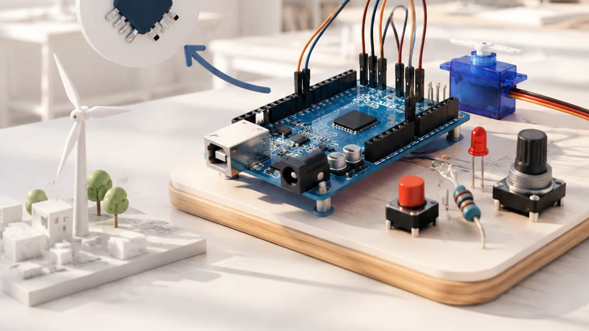
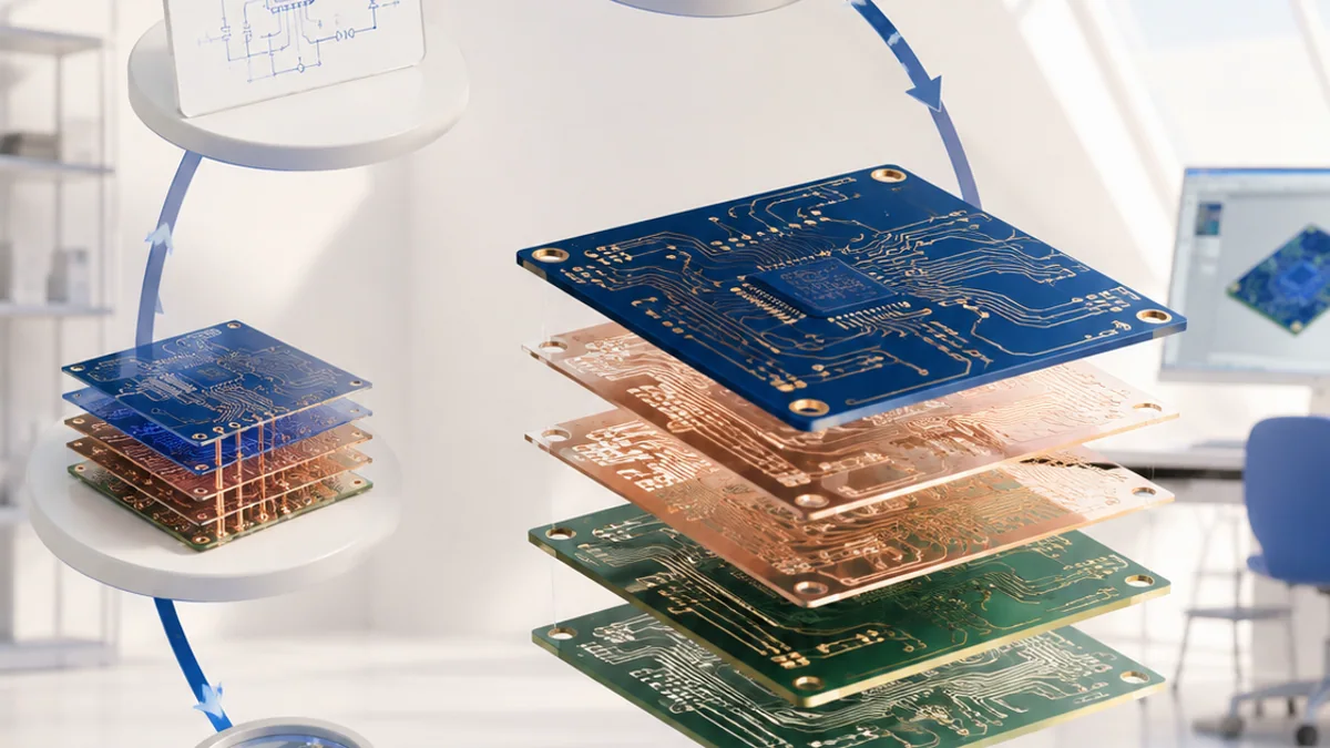
You can understand PCB Design without treating it as magic or memorizing a long list of terms. Start with one simple mental model, connect each part to an everyday example, and then add the technical details that make the system dependable.
The big idea: PCB design translates an electrical idea into exact physical layers that a manufacturer can build and inspect.
A beautiful layout cannot repair a wrong schematic. Check electrical intent before arranging the board.
Why this matters
A printed circuit board turns an electrical idea into a physical product. Good design keeps the meaning of the schematic while also respecting real component sizes, current paths and manufacturing limits.
By the end of this guide, you will be able to:
- Explain schematic symbols, nets, footprints and pads
- Place components using electrical and mechanical needs
- Route power, signals, planes and vias thoughtfully
- Run ERC and DRC before creating fabrication files
The goal is not only to recognize the words. It is to explain the system, predict what it will do, and design a small test that produces evidence.
1. From idea to schematic
The question: What information belongs in a schematic?
A schematic describes components and electrical connections, not their physical positions. Symbols represent parts, pins are connection points, and nets join pins that must be electrically common. Clear labels make intent reviewable.
Think of it like this: A subway map explains which stations connect even though it does not copy the city’s exact geography.
A concrete example
Draw a connector, resistor and LED in series; label power and ground and assign realistic values.
The flow: Requirement → Symbols → Nets and values → Electrical check
Try it yourself
- Draw a battery-resistor-LED schematic.
- Mark polarity and current path.
- Have a partner find one possible wiring error.
Quick check — Does schematic position determine board position?
No. The schematic shows electrical relationships; physical placement happens in the PCB layout.
2. Footprints and placement
The question: How does a symbol become a physical component?
A footprint contains copper pads and mechanical information that match a real part. Package dimensions, pin numbering and orientation must match the datasheet. Placement begins with board shape, connectors and mechanical constraints, then groups related components.
Think of it like this: A furniture plan must use the real dimensions and doorway positions, not just a list of furniture.
A concrete example
Place a decoupling capacitor close to the microcontroller power pin and keep connectors accessible at the edge.
The flow: Symbol → Datasheet package → Footprint → Placed component
Try it yourself
- Compare one symbol with two possible footprints.
- Use dimensions to choose the right one.
- Mark pin 1 on both.
Quick check — Why verify a footprint against the datasheet?
A wrong pad size, spacing or pin order can make the manufactured board unusable.
3. Copper, layers and routing
The question: How do physical tracks change circuit behaviour?
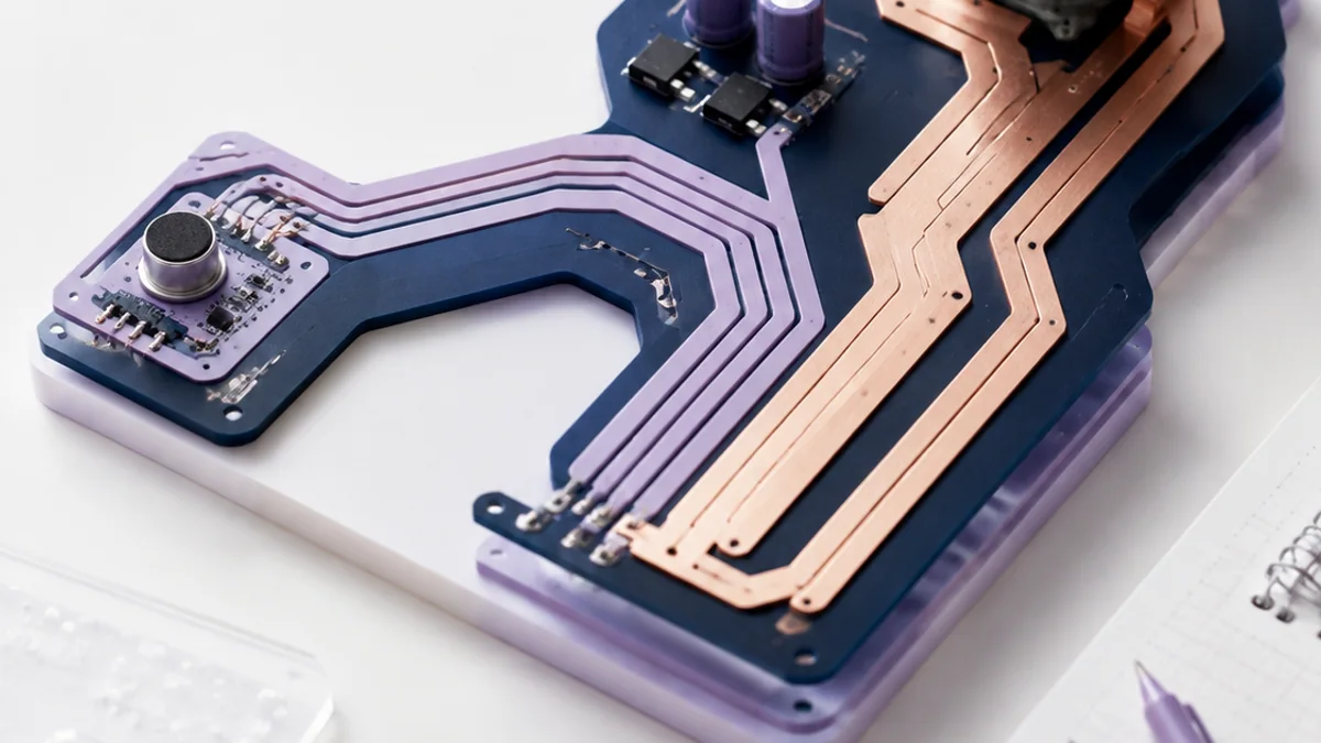
Tracks have resistance and carry current. Width, length, spacing and return path matter. Plan power first, use ground zones where appropriate, keep sensitive signals away from noisy switching paths, and use vias to change copper layers.
Think of it like this: Road width and route affect how much traffic can move and how different traffic streams interfere.
A concrete example
Use a wider power track for a motor load and keep its high-current return away from a small analog sensor path.
The flow: Place by function → Plan power → Route signals → Add return paths
Try it yourself
- Colour power, ground and signal nets differently on a printed layout.
- Find a long return path.
- Propose a shorter arrangement.
Quick check — What is a via?
A plated hole that electrically connects copper between PCB layers.
4. Checks and manufacturing output
The question: What should be verified before ordering a board?
Electrical Rules Check finds schematic conflicts; Design Rules Check finds layout violations. Inspect board outline, clearances, drill sizes, reference labels and polarity. Fabrication outputs commonly include Gerber layer files, drill data and assembly information.
Think of it like this: A building needs both design review and construction drawings before materials are cut.
A concrete example
Run ERC, update the PCB from the schematic, run DRC, inspect Gerbers in a viewer, then print the board at 1:1 scale to check connectors.
The flow: ERC → Update layout → DRC → Fabrication review
Try it yourself
- Create a pre-order checklist.
- Include electrical, mechanical and documentation checks.
- Explain who should review it.
Quick check — Why inspect Gerber files separately?
They are the actual layer data the manufacturer uses, so the review checks what will be fabricated.
Put the ideas together: Design a sensor indicator board
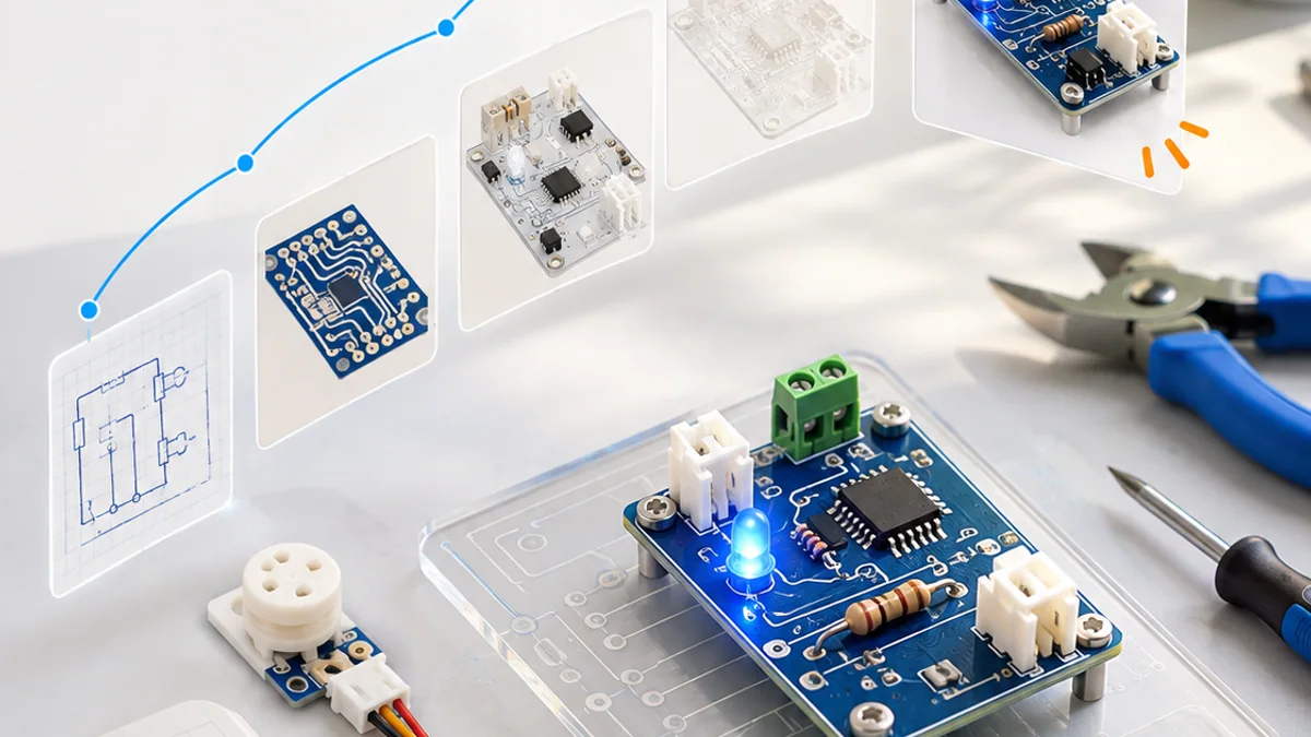
Create a beginner PCB plan with a power connector, sensor connector, resistor, LED and small controller.
Your build plan
- Capture and annotate the schematic.
- Select and verify footprints.
- Place connectors and related parts, then route.
- Run checks and review fabrication outputs.
Evidence to keep
- Schematic PDF or screenshot
- Annotated layout
- ERC and DRC results
- Manufacturing checklist
An engineer does not stop at “it worked once.” Keep the diagram, record the conditions, repeat the test, and note what changed between attempts.
Important safety and quality notes
- Use only safe low-voltage circuits for first boards.
- Check polarity, voltage ratings and connector pin order before power.
- Solder with ventilation, eye protection and a heat-safe stand.
The examples in this article are educational models. Check component ratings, manufacturer instructions, local rules and appropriate supervision before using real hardware.
Vocabulary without the jargon wall
| Term | Plain-language meaning |
|---|---|
| Schematic | A symbolic description of components and electrical connections. |
| Net | Pins that are intended to be electrically connected. |
| Footprint | The physical pad and outline pattern for a component. |
| Via | A plated connection between copper layers. |
| ERC | Electrical Rules Check for the schematic. |
| DRC | Design Rules Check for the board layout. |
What to remember
PCB design translates an electrical idea into exact physical layers that a manufacturer can build and inspect. The professional habit behind the technology is equally important: define the result, observe the system, measure what happened, and improve one thing at a time.
Continue with the full PCB Design learning path for the structured sessions, or explore the sources below when you are ready for deeper technical detail.
Sources and further learning
- KiCad documentation — KiCad
- Getting started in KiCad — KiCad
- PCB Editor manual — KiCad